AC Circuits and Electronics: From Basic Theory to Semiconductor Applications
Introduction to Alternating Current
Alternating current (AC) forms the foundation of modern electrical systems, from household power supplies to complex electronic devices. Unlike direct current (DC), AC voltage and current vary sinusoidally with time, creating unique characteristics that enable efficient power transmission and diverse applications in electronics.
When a coil rotates in a uniform magnetic field, the magnetic flux through the coil varies as φ = NBA cos ωt, where N is the number of turns, B is the magnetic field strength, A is the coil area, and ω is the angular frequency. This changing flux induces an electromotive force (EMF) given by e = -dφ/dt = NBAω sin ωt = e₀ sin ωt, where e₀ represents the peak voltage.
AC Circuit Analysis and Components
Resistive, Inductive, and Capacitive Circuits
In AC circuits, different components exhibit distinct phase relationships between voltage and current. For a pure resistor, voltage and current remain in phase, following Ohm's law with i = V/R sin ωt. However, reactive components introduce phase shifts that significantly impact circuit behavior.
Capacitive circuits demonstrate current leading voltage by π/2 radians (90 degrees). The capacitive reactance Xc = 1/(ωC) determines the opposition to current flow, where C represents capacitance and ω is the angular frequency. This relationship explains why capacitors block DC (infinite reactance at ω = 0) while allowing AC to pass more easily at higher frequencies.
Inductive circuits exhibit the opposite behavior, with current lagging voltage by π/2. The inductive reactance XL = ωL increases with frequency, making inductors effective at blocking high-frequency signals while allowing DC and low frequencies to pass with minimal opposition.
Impedance and Phasor Analysis
Complex AC circuits require impedance analysis to determine overall circuit behavior. Impedance Z combines resistance R with reactance components, calculated as Z = √[R² + (XL - Xc)²] for series RLC circuits. This vector relationship accounts for the phase differences between resistive and reactive components.
Phasor diagrams provide visual representation of these relationships, treating AC quantities as rotating vectors. This technique simplifies calculations and helps visualize phase relationships between multiple AC signals in complex circuits.
Resonance and Power in AC Circuits
Series Resonance Phenomenon
Series RLC circuits exhibit resonance when inductive and capacitive reactances cancel each other (XL = Xc). At the resonant frequency f₀ = 1/(2π√LC), impedance reaches its minimum value (equal to resistance R), resulting in maximum current flow. This condition finds applications in radio tuning circuits, filters, and oscillators.
The quality factor Q = ωL/R determines the sharpness of the resonance curve, indicating how selective the circuit is around the resonant frequency. Higher Q values produce sharper, more selective responses but with narrower bandwidth.
Power Relationships
AC power analysis involves three components: apparent power (VA), real power (W), and reactive power (VAR). The power factor cos φ represents the ratio of real power to apparent power, where φ is the phase angle between voltage and current. Unity power factor (cos φ = 1) indicates maximum power transfer efficiency, while zero power factor represents purely reactive circuits with no net power consumption.
Average power consumption in AC circuits follows Pav = VrmsIrms cos φ, emphasizing the importance of power factor in electrical efficiency. Poor power factor necessitates larger currents to deliver the same real power, increasing transmission losses and equipment requirements.
Transformers and Power Transfer
Transformers enable efficient voltage transformation in AC systems through electromagnetic induction. The voltage relationship Vp/Vs = Np/Ns, where subscripts p and s denote primary and secondary windings respectively, allows stepping voltage up or down based on turns ratio. Ideal transformers conserve power, so current relationships follow Ip/Is = Ns/Np.
Step-up transformers (Ns > Np) increase voltage while decreasing current, enabling efficient long-distance power transmission. Step-down transformers reduce voltage for safe consumer applications. The inability of transformers to operate with DC stems from the requirement for changing magnetic flux to induce secondary voltage.
Semiconductor Physics and Devices
Intrinsic and Extrinsic Semiconductors
Pure semiconductors like silicon and germanium exhibit energy gaps between valence and conduction bands that allow controlled conductivity. At room temperature, thermal energy promotes some electrons from the valence band to the conduction band, creating electron-hole pairs that enable current flow.
Doping introduces controlled impurities to modify semiconductor properties. N-type doping with pentavalent atoms (phosphorus, arsenic) provides excess electrons, while P-type doping with trivalent atoms (boron, aluminum) creates electron deficiencies or "holes." These modifications dramatically alter conductivity and enable the creation of electronic devices.
PN Junctions and Diodes
PN junctions form the basis of most semiconductor devices. The boundary between P-type and N-type materials creates a depletion region where mobile charge carriers are absent. This region acts as a potential barrier, allowing current flow in only one direction under normal conditions.
Forward bias reduces the depletion layer thickness, enabling current flow, while reverse bias widens the depletion region, blocking current. This unidirectional behavior makes PN junctions ideal for rectification, converting AC to DC through half-wave or full-wave rectifier circuits.
Transistor Operation and Amplification
Bipolar Junction Transistors
Transistors consist of three semiconductor regions forming either NPN or PNP configurations. The base region, typically very thin (3-5 micrometers), controls current flow between emitter and collector. Small base current variations produce large collector current changes, providing current amplification.
The current relationships IE = IB + IC and the current gain β = IC/IB characterize transistor operation. Common-emitter configuration provides both current and voltage gain, making it popular for amplifier applications. The relationship α = IC/IE (typically 0.9-0.99) represents the fraction of emitter current reaching the collector.
Amplifier Design
Transistor amplifiers require proper biasing to establish operating points in the active region. The common-emitter amplifier demonstrates voltage gain Av = -βRL/ri, where RL is the load resistance and ri is the input resistance. The negative sign indicates phase inversion between input and output signals.
Power gain combines current and voltage gains: Ap = (β²RL)/(ri), showing how transistors can provide significant power amplification for weak input signals. Proper selection of bias points and load resistances optimizes amplifier performance for specific applications.
Essential AC Circuit and Electronics Formulas
| Formula Name | Mathematical Expression | Description |
|---|---|---|
| AC Voltage | e = e₀ sin ωt | Sinusoidal voltage variation with time |
| RMS Value | Vrms = V₀/√2 | Root mean square value for AC quantities |
| Capacitive Reactance | Xc = 1/(ωC) | Opposition to AC current in capacitors |
| Inductive Reactance | XL = ωL | Opposition to AC current in inductors |
| Impedance (RLC) | Z = √[R² + (XL - Xc)²] | Total opposition in AC circuits |
| Resonant Frequency | f₀ = 1/(2π√LC) | Frequency of series resonance |
| Power Factor | cos φ = R/Z | Ratio of real to apparent power |
| Average Power | Pav = VrmsIrms cos φ | Real power consumption in AC circuits |
| Transformer Ratio | Vp/Vs = Np/Ns | Voltage transformation relationship |
| Current Gain (BJT) | β = IC/IB | Transistor current amplification factor |
| Voltage Gain (CE) | Av = -βRL/ri | Common-emitter voltage amplification |
| Semiconductor Conductivity | σ = (neμe + nhμh)e | Conductivity in terms of charge carriers |
Practical Applications and Modern Relevance
AC circuit principles underpin countless modern technologies, from power generation and distribution to wireless communication systems. Understanding impedance matching ensures maximum power transfer in RF applications, while resonance principles enable selective filtering in communication circuits.
Semiconductor devices have revolutionized electronics, enabling everything from simple diodes to complex integrated circuits. The progression from basic PN junctions to sophisticated transistor amplifiers demonstrates the fundamental importance of semiconductor physics in modern technology.
These concepts continue evolving with advances in materials science and circuit design, making solid understanding of AC circuit theory and semiconductor physics essential for engineers and students working with electrical and electronic systems.
ALTERNATING CURRENT
Basic Concepts
Flux linked with any coil in a uniform magnetic field is given by: φ = N BA sin θ
If a coil of area A placed in uniform magnetic field B is rotated with constant angular velocity ω, the flux at any time through the coil is: φ = N BA cos ωt
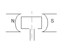
Therefore induced emf:
e = -dφ/dt = N BA ω sin ωt = e₀ sin ωt
where e₀ = N BA ω
This sinusoidally varying voltage is known as AC voltage.
Mean Value of Voltage and Current
For sinusoidal AC: I = I₀ sin ωt
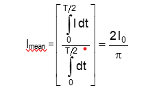
Similarly:
V_mean = (2V₀)/π
Root Mean Square (RMS) Values
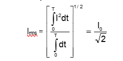
Similarly: V_rms = V₀/√2
IMPEDANCE
In any circuit, the ratio of the effective voltage to the effective current is defined as the impedance Z of the circuit.
Its unit is ohm.
PHASORS AND PHASOR Diagrams
In the study of A.C. circuits, we encounter alternating voltage and currents which have the same frequency but differ in phase with each other. It is found that the study of A.C. circuits becomes quite easy if alternating currents and voltages are treated as vectors or more correctly as 'phasors'.
A diagram representing alternating voltage and current as vectors with the phase angle between them is called a phasor diagram.
AC CIRCUIT COMPONENTS
A resistor in an AC circuit
i = E/R = (e₀/R) sin ωt = i₀ sin ωt
where i₀ = e₀/R
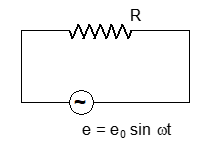
In a resistor, voltage and current are in phase.
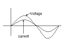
A capacitor in an AC circuit
Q = CV = Ce₀ sin ωt
I = dQ/dt = ωCe₀ cos ωt
= i₀ cos ωt = i₀ sin (ωt + π/2)
where i₀ = ωCe₀ = e₀/X_C
X_C = 1/(ωC) is known as capacitive reactance
In a capacitor, voltage leads the current (or current lags the voltage) by π/2.
An inductor in an AC circuit
e = inductor in an ac circuit
e = e₀ sin ωt = L di/dt
i = -(e₀/ωL) cos ωt = -i₀ cos ωt = i₀ sin (ωt - π/2)
where i₀ = e₀/(ωL) = e₀/X_L
X_L = ωL is known as inductive reactance
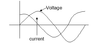
In an inductor, current lags the voltage by π/2.
COMBINATION OF ALL THREE (RLC CIRCUIT)
For RLC series circuit:
.png)
.png) wo
wo
V = V_R + V_L + V_C (vector addition)
V = √[V_R² + (V_L - V_C)²] = I√[R² + (X_L - X_C)²]
where X_L = ωL and X_C = 1/(ωC)
V = IZ, where Z = √[R² + (X_L - X_C)²] is the impedance
Phase Angle
tan φ = (X_L - X_C)/R = (V_L - V_C)/V_R
Phase Relationships
- When ωL > 1/(ωC): tan φ is positive, EMF leads current
- When ωL < 1/(ωC): tan φ is negative, EMF lags current
- When ωL = 1/(ωC): tan φ is zero, current and EMF are in phase
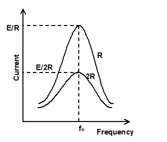
- When ωL = 1/(ωC): impedance equals R (minimum), current is maximum - this is RESONANCE
Resonance
ω₀ = 1/√(LC) where ω₀ is resonant frequency
f₀ = 1/(2π√(LC))
Series resonant circuit is also called acceptor circuit.
If R, L and are constant, and the frequency f of the applied emf is raised continuously from zero, the peak current varies as shown in figure. At first the current is very small, increases to maximum when the frequency increase to it's resonance value of, and then falls again.
It is interesting to note that before resonance the current leads the applied emf, at resonance it is in phase, and after resonance it lags behind the emf. Series resonant circuit is also called acceptor circuit.
POWER IN AC CIRCUITS
e = e₀ sin ωt
I = i₀ sin (ωt - φ) where -90° ≤ φ ≤ 90°
P = e₀ i₀ sin ωt sin (ωt - φ)
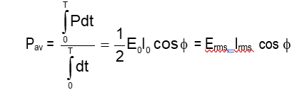
Where cos φ is known as power factor.
Wattless Current
If cos φ = 0, or φ = π/2, then P_av = 0
When current and voltage differ in phase by 90°, this case is known as wattless current, because the average power consumed in the circuit is zero.
Transformers
e_p/e_s = N_p/N_s
Where e_p and e_s are voltages in primary and secondary, and N_p and N_s are number of turns in primary and secondary coils.
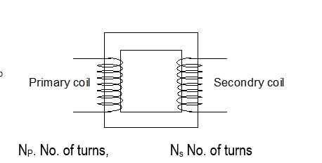
Types of Transformers
- Step-up transformer: If e_p > e_s such that N_p > N_s
- Step-down transformer: If e_s > e_p such that N_s > N_p
Exercise Questions:
- (i) A voltmeter attached to a.c. supply reads which voltage (peak voltage, rms voltage or mean voltage)?
- (ii) Through what a.c. components can wattless current be attained?
- (iii) Why do transformers not work when d.c. voltage is applied?
Detailed Illustration Examples:
Example 1:
Problem: A 0.21 H inductor and 12 ohm resistance connected in series to 220V, 50Hz AC source. Calculate current and phase angle.
Solution:
X_L = ωL = 2πfL = 2π × 50 × 0.21 = 21π Ω
Z = √(R² + X_L²) = √(12² + (21π)²) = √(144 + 4348) = √4492 = 67.02 Ω
I = V/Z = 220/67.02 = 3.28 A
φ = tan⁻¹(X_L/R) = tan⁻¹(21π/12) = tan⁻¹(5.5) = 79.7°
Current lags voltage by 79.7°
Example 2:
Problem: Series LCR circuit with R = 120Ω, angular resonance frequency 4×10⁵ rad/s. At resonance, V_R = 60V, V_L = 40V. Find L and C.
Solution:
At resonance: I = V_R/R = 60/120 = 0.5 A
V_L = IX_L = IωL, so L = V_L/(Iω) = 40/(0.5 × 4×10⁵) = 2×10⁻⁴ H
At resonance: ωL = 1/(ωC), so C = 1/(ω²L) = 1/((4×10⁵)² × 2×10⁻⁴) = 1/(32×10⁶) = 1/(32) × 10⁻⁶ F
CHOKE COIL
The current in an A.C. circuit can be reduced by using a resistor or a choke coil. The use of resistor is associated with a loss of energy (i²R), therefore the use of choke coil is preferred as it does not employ any power loss.
A choke coil is a coil of insulated copper wire which offers a high reactance (ωL) to A.C. (but a low D.C. resistance), thus reducing the A.C. appreciably without the loss of energy.
The average power consumed in A.C. circuit is:
P = (E₀I₀/2) cos φ
The power factor is given by:
cos φ = R/√(R² + (ωL)²) = R/√((Lω)² + R²)
The inductance 'L' of the choke coils is quite large due to its large number of turns and high permeability of iron core, while resistance R is very small. In pure inductance cos φ = 0, but practically cos φ ≠ 0, therefore power absorbed by coil is extremely small. Thus choke coil reduces current without appreciable loss of energy. The wastage is only due to hysteresis loss in soft iron core. Eddy current loss is reduced by laminating the soft iron core.
ELECTRONICS
SEMICONDUCTORS
Concepts of Metals, Insulators and Semi-Conductors
The difference between metals, insulators and semi-conductors is essentially a difference in the energy gap between the valence band and conduction band.
| Material Type | Energy Gap | Description |
|---|---|---|
| Conductor | E_G << kT | Valence and conduction bands overlap |
| Semiconductor | E_G ~ kT | Small energy gap |
| Insulator | E_G >> kT | Large energy gap |
Energy Bands
- The energy band formed by valence electrons of an atom is known as valence band.
- The next energy band after the valence band available for electrons to occupy is called the conduction band.
- The difference between metals, insulators and semiconductors is the energy gap between valence and conduction bands.
Intrinsic Semi-Conductors
Silicon atom with electronic configuration 1s² 2s² 2p⁶ 3s² 3p² has 4 valence electrons. It forms four bonds in a tetrahedral configuration with four neighboring Si atoms.
At room temperature, some electrons have sufficient energies to break bonds and move freely to the conduction band. The electrons that leave create vacancies called holes. An electron-hole pair is created.
Current in Semiconductors
- Electron current: Electrons in conduction band conduct under electric field
- Hole current: Holes appear to move when electrons fill vacancies
σ = J/E = ne(v/E) = neμ, where μ is called mobility
Total current = electronic current + hole current
σ = n_e·e·μ_e + n_h·e·μ_h
Exercise 2:
What is the difference between an electron in a doped semiconductor and the electron in a hydrogen atom?
Extrinsic Semi-Conductors
N-type Semiconductors
- Add Group V impurities (like Phosphorus) to intrinsic semiconductor
- Phosphorus is pentavalent - four electrons bond in Si matrix, fifth electron is in donor level
- Fifth electron requires little energy to escape to conduction band
- Electrons are majority carriers
P-type Semiconductors
- Add Group III impurities (like Aluminum) to intrinsic semiconductor
- Aluminum is trivalent - three electrons bond in matrix, fourth bond has a hole
- Holes are in acceptor level
- Electrons from valence band can easily reach these holes
- Holes are majority carriers
PN Junction
P and N semiconductors are joined together to form PN junctions. It behaves as a diode.
Depletion Layer
Near the junction, electrons diffuse from N-type to occupy holes in P-type. This creates a layer without carriers called the depletion layer.
Currents in PN Junction
- Diffusion current: Flow of majority carriers from higher to lower concentration
- Drift current: Flow due to electron-hole pairs created in depletion region
Biasing Conditions
- Unbiased: Diffusion current = Drift current, net current = 0
- Forward biased: Diffusion current increases, depletion layer becomes thin
- Reverse biased: Depletion layer widens, diffusion current decreases
PN Junction as a Rectifier
Half Wave Rectifier
Uses a single diode to convert AC to pulsating DC. Only one half of the AC waveform passes through.
Full Wave Rectifier
Uses multiple diodes to convert both halves of AC waveform to DC, resulting in better efficiency.
TRANSISTORS
Transistors are semiconductor devices capable of power amplification and having three leads. They consist of a thin central layer of one type of semiconductor between two relatively thick pieces of the other type.
Types of Transistors
- npn transistor: Thin p-type material between two n-type pieces
- pnp transistor: Thin n-type material between two p-type pieces
Transistor Terminals
- Emitter: One end piece
- Base: Central thin layer (lightly doped, 3-5 μm thick)
- Collector: Other end piece
Operating States
| State | Emitter-Base Junction | Base-Collector Junction |
|---|---|---|
| Active | Forward Biased (FB) | Reverse Biased (RB) |
| Cut-off | Reverse Biased (RB) | Reverse Biased (RB) |
| Saturation | Forward Biased (FB) | Forward Biased (FB) |
Current Relations
Using Kirchoff's current law:
I_E = I_B + I_C
Important Parameters
- α = I_C/I_E (close to 0.9)
- β = I_C/I_B (order of 100 or more)
Relations:
- α = β/(1 + β)
- β = α/(1 - α)
Transistor as an Amplifier
For amplification:
- Emitter-base junction: Forward biased (FB)
- Base-collector junction: Reverse biased (RB)
Common Emitter Amplifier
Load is connected between collector and DC supply.
AC input signal v_s is superimposed on bias V_BE.
Key Relations
- v_s = ΔV_BE = r_i ΔI_B
- β_ac = ΔI_C/ΔI_B (current gain factor)
- v_o = ΔV_CE = -R_L ΔI_C = -β_ac R_L ΔI_B
Voltage Gain
A_v = v_o/v_i = (ΔV_CE/ΔV_BE) = -(β_ac R_L)/r_i = -g_m R_L
where g_m = β_ac/r_i is transconductance
Detailed Working Example:
For Common Emitter amplifier:
- v_s = ΔV_BE = r_i ΔI_B
- ΔI_C = β_ac ΔI_B
- v_o = ΔV_CE = -R_L ΔI_C = -β_ac R_L ΔI_B
- A_v = v_o/v_s = (-β_ac R_L ΔI_B)/(r_i ΔI_B) = -β_ac R_L/r_i
FORMULAE AND CONCEPTS AT A GLANCE
1. For sinusoidal AC:
- I_av = (2I_0)/π = 0.636I_0
- I_rms = I_0/√2 = 0.707I_0
- V_av = (2V_0)/π = 0.636V_0
- V_rms = V_0/√2 = 0.707V_0
2. Reactances:
- X_C = 1/(ωC)
- X_L = ωL
3. For RLC circuit:
Z = √[R² + (X_L - X_C)²]
4. At resonance:
- ω = 1/√(LC)
- f = 1/(2π√(LC))